
Intel has been talking about its upcoming 22nm chip manufacturing technology for a while now but while out at IDF we were given an in-depth briefing on just what Intel has been working on and what it means for chip designs of the future.
For those unfamiliar, 22nm refers to the width of the transistors used in the design of microprocessors. As the size of these transistors is reduced through technological advancements, the size of the overall chip is reduced and its power consumption generally drops too thanks to less voltage being needed to power the smaller transistors.

The pace of innovation and drive to keep on reducing chip size has been so steady that it prompted Gordon Moore to propose that the number of transistors that will fit in any given space of silicon will double every two years. 56 years on this has stayed largely true with just the last eight years seeing the industry move from 90nm through 65nm and 45nm, and onto today’s standard of 32nm.
The next step is to 22nm but unlike the Taiwanese Semi-Conductor Manufacturer (TSMC) and Global Foundries, Intel has decided not to simply shrink the current standard chip design – called the planar transistor – but use a new type of transistor.
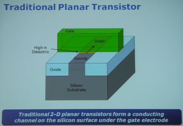
Traditional, planar, transistors form a conducting channel (the bit across which current flows to say the transistor is on) from a single flat surface below the gate (the bit that switches current flow on and off). But with tri-gate the new design has the silicon upon which the conducting surface is formed project up into the gate, providing contact on three sides.

The result is a conducting surface that is as effective as a much wider one on a planar design. This allows the designs to be smaller without increasing current leakage (the number one enemy for power consumption).
Editorial independence
Editorial independence means being able to give an unbiased verdict about a product or company, with the avoidance of conflicts of interest. To ensure this is possible, every member of the editorial staff follows a clear code of conduct.
Professional conduct
We also expect our journalists to follow clear ethical standards in their work. Our staff members must strive for honesty and accuracy in everything they do. We follow the IPSO Editors’ code of practice to underpin these standards.