Verdict
Key Specifications
- Review Price: £425.00
The release of the G80 based nVidia GeForce 8800 GTX in November 2006 was, in hindsight, a paradigm shift in the computer graphics world. Not only was it the first DirectX 10 graphics card but it also completely blew away the competition in DirectX 9 games before the arrival of Windows Vista and held this lead for an unprecedented amount of time even when Vista and DirectX 10 did finally arrive. Indeed, not until February of this year, when AMD released the ATI Radeon HD 3870 X2, which used two RV670 cores on one card, did the G80 in its various guises have any real competition.
Not that this competition lasted long. Within a few weeks nVidia released the dual G92 based 9800 GX2, which used a similar two-chips-on-one-card method to the HD 3870 X2, and comfortably regained the top performance crown – at least in the games it worked with. nVidia then followed this up with the 9800 GTX, which used a single G92 based chip to marginally extend nVidia’s performance lead within the single-chip graphics card market. Of course, ATI still had many good cards and it competed very fiercely in the mainstream sub-£150 market but it just couldn’t claim the top spot.
Still, while nVidia held onto its lead with the 9800 series cards, it didn’t really push forward any frontiers. Performance was good but not overwhelming and, while new features like HybridPower are useful, the whole range felt a little disappointing. 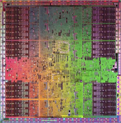
Just a few months later, though, nVidia has just launched a brand new graphics processor called GT200 that, at least on paper, looks like it should have all the performance necessary to be a true successor to G80. Made up of 1.4 Billion (yes, that is billion with a ‘B’) transistors, packing in 240 stream processors, 32 ROPs, a 512-bit memory interface, and a whole host of other under-the-bonnet improvements, it is an absolute monster. In fact, with it still being made using the same 65nm process used on G92, it is not just a monster internally, but also externally – at 24 x 24mm this is the biggest single die TSMC has ever commercially produced.
Indeed, if you look at a typical production silicon wafer, which is 300mm in diameter, at most there is only room to produce 94 GT200 chips on each one. Compare this to something like Intel’s Conroe CPUs, which are built on the same size manufacturing process but are only 143mm^2 in size, so 426 dies can be produced per wafer, and you get some idea for just how large and expensive GT200 is.
Two variants on the GT200 will be available at launch, and these will be the first parts to take on nVidia’s revised branding. All the rebranding boils down to is the switching around of letters and numbers so the new cards are called GTX 280 and GTX 260 rather than the x000 GT/GTX/GTS sort of arrangement we’re used to.
The GTX 280 will use the full extent of GT200 with its shader clock running at 1296MHz, 1GB GDDR3 memory running at 1107MHz (2.2GHz effectively), and the rest of the chip purring away at 602MHz. As the power requirement for all this lot will be 236W, the GTX 280 will not only need a conventional six-pin PCI-Express connector but an extra eight-pin one as well.
Meanwhile, the GTX 260, which will be released on the 26th of June (the GTX 280 will be available by the time you read this), has two SM clusters disabled (I’ll explain more about this on the next page) and one ROP partition has also been removed. As well as this the clock speeds have been throttled resulting in vital statistics of: 192 shaders running at 1242MHz, 28 ROPs running at 576MHz, and 896MB GDDR3 1000MHz memory. As a result of these speed and component cuts, the GTX 260 will draw less power, 183W to be exact, and consequently needs only a single six-pin PCI-Express power connector. 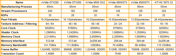
List pricing is as astronomical as you would expect with the GTX 280 demanding £449 and the GTX 260 £299. What’s more, early indications suggest this pricing won’t be deviated from too much by stores running discounts or trying to out-price each other. Nevermind, hey.
We’ll take a proper look at the GTX260 in a separate article and we’ll have a poke around the physical GTX280 card in a few moments but first let’s look at what makes nVidia’s latest graphical wonder tick.
Although GT200’s architecture is in many ways very similar to that of G80, there is a huge number of tweaks that have been applied to this new core that make it a considerably better whole. Before we get too far into the comparisons, though, let’s get back to basics.
The following is a Streaming Multiprocessor, or SM as nVidia abbreviates it to: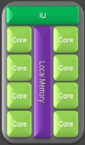
As you can see from the picture, an SM is an array of processing cores called Streaming Processors (SPs), with a portion of cache memory and an instruction scheduler. There’s actually a bit more to it than that, including two Special Function Units (SFU) that aren’t pictured, but we won’t go too far into the specifics. Essentially, this little lot acts like a mini eight core CPU with each core performing the calculations associated with a single pixel. The small (16KB) portion of memory is used to handle only the specific data associated with those eight pixels the SM is currently working on. This is the basic building block of nVidia’s unified shader architecture and is the same on both the G80, G92 and GT200. 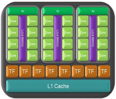
(centre)”TPC from GT200”(/centre)
As we zoom out one step we see the first major dividing point between G80/G92 and GT200. In GT200, three of these SMs are combined to form a Texture/Processor Cluster (TPC), whereas G80 and G92 used two SMs per TPC. The principle’s the same, there’s just more in the new chip – 32 SPs vs. 24 on G80. 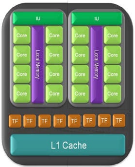
(centre)”TPC from G80/G92”(/centre)
As well as combining the SMs, a TPC also adds texture processing capabilities and again this is another area where the new chip differs from its forebears, sort of. On G80 you got four texture address units and eight texture filtering units per TPC, with G92 the number of address units doubled to eight while filtering remained at eight units. Now, with GT200 things have, well, stayed the same.
You still get eight texture address units and eight filtering units per TPC, it’s just the ratio of shaders to texturing units has changed. So, while the shader count of each TPC has increased by 50 per cent, the texturing power of each TPC has remained the same. At first this may seem like a backward step but most modern games are becoming shader dependent so the change in ratio makes sense. Moreover, when you look at the bigger picture you’ll see that the total texturing power of GT200 has actually increased a small amount.
What can we say about Counter-Strike: Source that hasn’t been said before? It is simply ”the” benchmark for team-based online shooters and, four years after its release, it’s still one of the most popular game in its genre. In complete contrast to Enemy Territory: Quake Wars, it focuses on small environments and incredibly intensive small-scale battles with one-shot kills the order of the day. If you want to test all elements of your first person shooter skills in one go, this is the game to do it.
We test using the 32-bit version of the game using a custom timedemo taken during a game against bots on the cs_militia map. This has a large amount of foliage, so transparency antialiasing has a significant impact on image quality and performance, and is generally one of the most graphically intensive maps available. We find a framerate of at least 60fps is required for serious gaming as this game relies massively on quick, accurate reactions that simply can’t be compromised by dropped frames.
All in-game settings are set to their maximum and we test with 0xAA 0xAF, 2xAA 4xAF, and 4xAA 8xAA. Transparency anti-aliasing is also manually turned on through the driver, though this is obviously only enabled when normal AA is being used in-game.
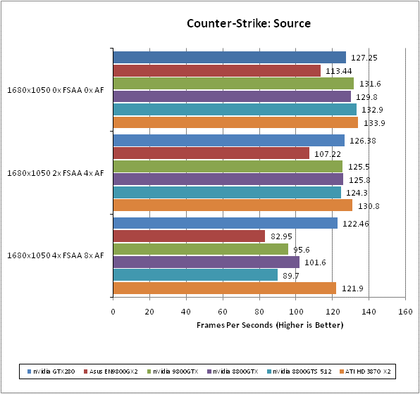
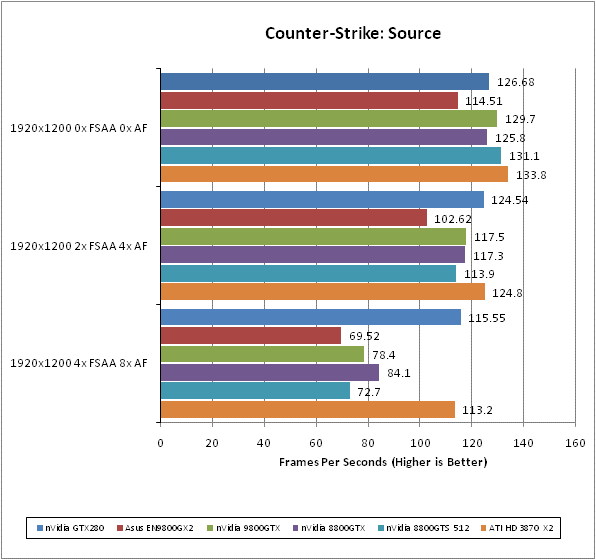
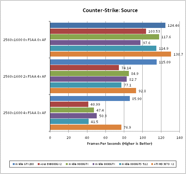
Although ATI’s HD 3870 X2 makes a good go of keeping up with GTX280, when it comes to the crunch it simply can’t match nVidia’s latest. Once again, GTX280 reigns supreme.
Call of Duty 4 has to be one of our favourite games of last year. It brought the Call of Duty brand bang up to date and proved that first person shooters didn’t need to have the best graphics, or the longest game time. It was just eight hours of pure adrenaline rush that constantly kept you on edge.
We test using the 32-bit version of the game patched to version 1.4 FRAPS is used to record framerates while we manually walk through a short section of the second level of the game. We find a framerate of 30fps is quite sufficient because, although the atmosphere is intense, the gameplay is less so – it doesn’t hang on quick reactions and high-speed movement.
All in-game settings are set to their maximum and we test with 0xAA and 4xAF. Transparency anti-aliasing is also manually turned on through the driver, though this is obviously only enabled when normal AA is being used in-game.
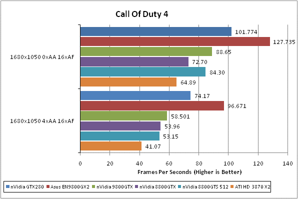
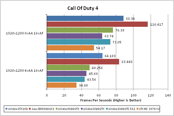
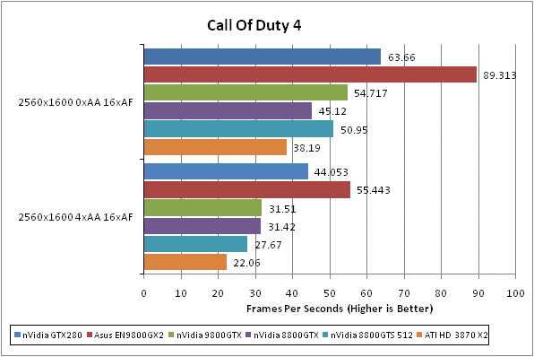
For some reason this game simply didn’t benefit that much from the various improvements made to GT200 and it is simply trounced by the 9800 GX2. We suspect this is largely due to Call of Duty 4 being a DirectX 9 based game so it is benefiting little from the more DirectX 10 orientated tweaks applied to GT200. It still runs absolutely fine though.
Enemy Territory: Quake Wars distinguishes itself from all our other tests by the fact it uses the open source OpenGL API rather than Microsoft’s DirectX. It’s a team-based first person shooter set in a dystopian future war scenario. As a player you get to choose from an enormous range of character types and playing styles, and there’s a whole host of vehicles to choose from too. Battles can span vast areas of open space and involve a huge number of participants. All in all, it’s multiplayer heaven.
We test using the 32-bit version of the game, which is patched to version 1.4. We use a custom timedemo from the Valley level, which we feel is about as graphically intensive as the game gets. We feel a framerate of at least 50fps is required for this game as the intense multiplayer action and high speed mouse movement demands it.
All in-game settings are set to their maximum and we test with 0xAA 0xAF, 2xAA 4xAF, and 4xAA 8xAA. Transparency anti-aliasing is also manually turned on through the driver, though this is obviously only enabled when normal AA is being used in-game.
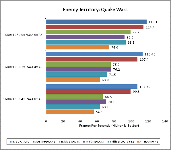
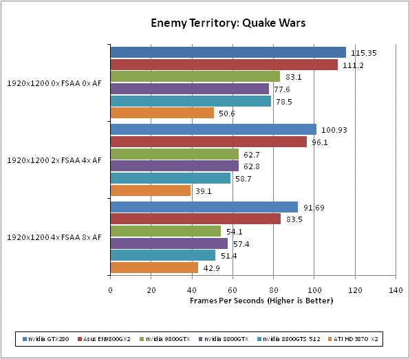
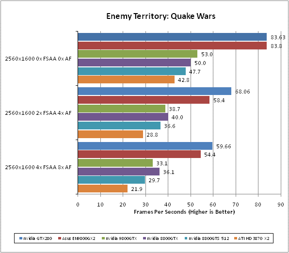
The positive story continues with Enemy Territory – GTX280 simply blows away everything else. Even the 9800 GX2 consistently has to play second fiddle and this is a game that scales very well in SLI.
Race Driver: GRID is the newest game in our testing arsenal and it’s currently one of our favourites too. Its combination of arcade style thrills and spills with a healthy dose of realism and extras like Flashback makes it a great pickup and go driving game. It’s also visually stunning with beautifully rendered settings, interactive crowds, destructible environments, and stunning lighting. All that and it’s not the most demanding game on hardware, either.
We test using the 32-bit version of the game, which is unpatched and running in DirectX10 mode. FRAPS is used to record frame rates while we manually complete one circuit of the Okutama Grand Circuit, in a Pro Tuned race on normal difficulty. We find a framerate of at least 40fps is required to play this game satisfactorily as significant stutters can ruin your timing and precision. We’d also consider 4xAA as a minimum as the track, barriers, and car bodies suffer considerably from aliasing and are a constant distraction.
All in-game settings are set to their maximum and we test with 0xAA, 4xAA, and 8xAA. Transparency anti-aliasing is also manually turned on through the driver, though this is obviously only enabled when normal AA is being used in-game.
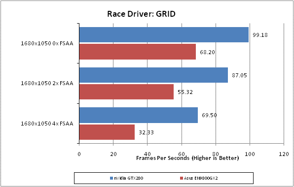
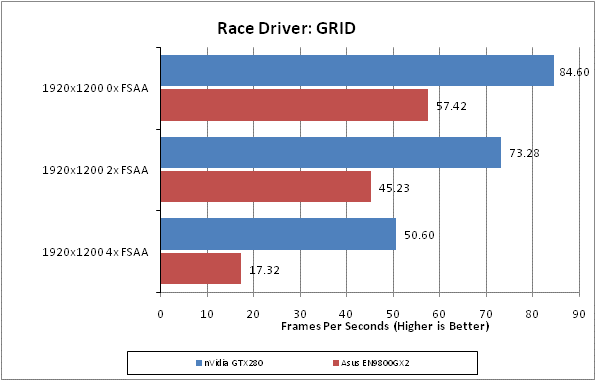
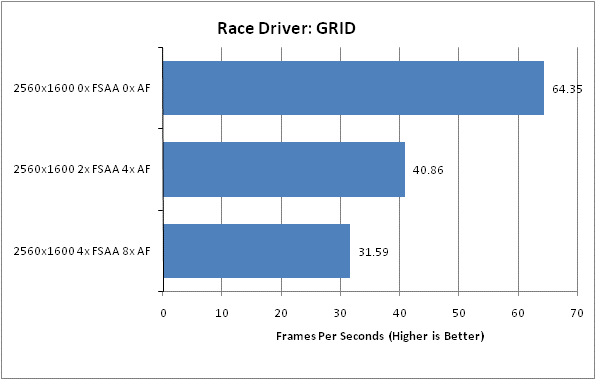
We had very limited time to test this game so we only got comparable results on a couple of cards. It’s also clear that nVidia hasn’t had a chance to optimise its SLI drivers for this game as the 9800 GX2 struggles more than it should. All told, then, we can’t comment on the big picture. However, even with limited testing it is quite clear that GTX280 is a great choice for playing this game.
While it hasn’t been a huge commercial success and its gameplay is far from revolutionary, the graphical fidelity of Crysis is still second to none and as such it’s still the ultimate test for a graphics card. With masses of dynamic foliage, rolling mountain ranges, bright blue seas, and big explosions, this game has all the eye-candy you could wish for and then some.
We test using the 32-bit version of the game patched to version 1.1 and running in DirectX 10 mode. We use a custom timedemo that’s taken from the first moments at the start of the game, wondering around the beach. Surprisingly, considering its claustrophobic setting and graphically rich environment, we find that any frame rate above 30fps is about sufficient to play this game.
All in-game settings are set to high for our test runs and we test with both 0xAA and 4xAA. Transparency anti-aliasing is also manually turned on through the driver, though this is obviously only enabled when normal AA is being used in-game.
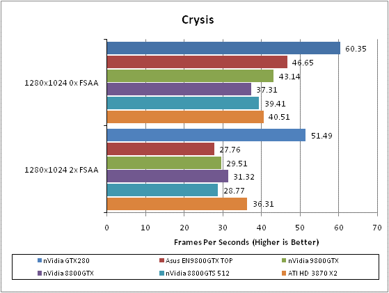
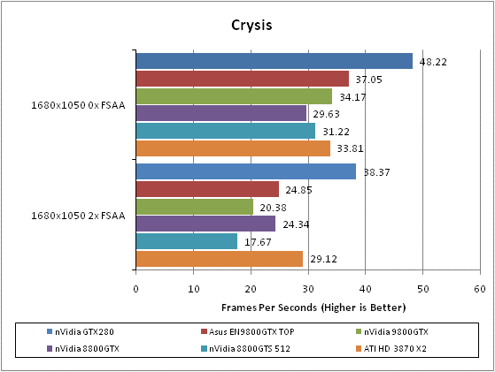
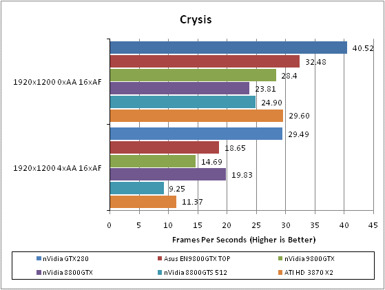
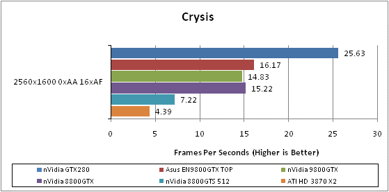
There’s not much to say here, really. GTX280 is by far the best bet for playing Crysis. In fact, it’s the first card we’ve seen that makes this game playable at 2,560×1,600. This is a great start.
As I alluded to earlier, the GTX280 launch has coincided with a massive push on nVidia’s part to promote GPGPU. However, while this may be interesting it is still far from being of great significance to anyone looking to by one of these cards. So, until the whole GPGPU spectrum evens out and we get some sort of standards coming into play we will leave analysis of GPGPU performance out of the equation. So, let’s get those games fired up instead.
”’Common System Components”’
* Intel Core 2 Quad QX9770
* Asus P5E3
* 2GB Corsair TWIN3X2048-1333C9 DDR3
* 150GB Western Digital Raptor
* Microsoft Windows Vista Home Premium 32-bit
”’Drivers”’
* GTX280: Forceware 177.34
* Other nVidia cards: Forceware 175.16
* ATI: Catalyst 8.4
”’Cards Tested”’
* nVidia GeForce GTX 280
* nVidia GeForce 9800 GTX
* nVidia GeForce 9800 GX2
* nVidia GeForce 8800 GTX
* nVidia GeForce 8800 GTS 512
* ATI HD 3870 X2
”’Games Tested”’
* Crysis
* Race Driver: GRID
* Enemy Territory: Quake Wars
* Call of Duty 4
* Counter-Strike: Source
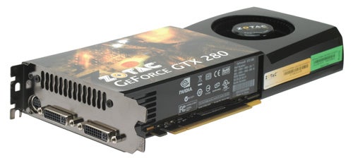
The first card we were provided with for review is made by Zotac but apart from the Zotac sticker it is the exact same design as nVidia’s reference board so that’s what we will be basing our assessment on. We will address the specifics of the Zotac board along with a number of other partner cards when we do a roundup soon. 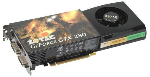
The GTX280 card is 267mm long, which is roughly the same length as the 9800 GX2. Also like the GX2, it is completely enclosed by a metal shroud. This protects the delicate electronics from potential damage due to static or general knocks and scrapes and is a development we welcome with open arms.
Again like all nVidia’s recent high-end cards, GTX280 uses a dual-slot heatsink/fan design that employs the slightly off-parallel fan alignment that debuted with the 8800 GTS 512. As we’ve come to expect, the cooler is very effective with it remaining near silent when idle and although it gets loud when under load it is a gentle whoosh rather than a high-pitched squeal or annoying buzz. The card does get very hot and will require a well ventilated case to ensure it doesn’t cause stability problems but, again, this is something we would fully expect from a high-end graphics card. 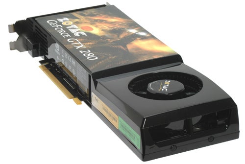
As mentioned, the peak power draw is a hefty 236W. However, this is a worst case scenario and nVidia has employed some great power saving measures that result in idle power being a mere 25W and power draw during accelerated video playback will only rise to 32W. These are very impressive figures that do make you wonder about the merits of HybridPower, especially as we’ve found the chipsets that support this power saving feature consume significant amounts of power themselves.
Even though the card ”can” draw very little power, it still won’t work without both auxiliary PCI-Express power sockets correctly connected – something that will be made obvious by an LED on the expansion bracket, which glows red if the card hasn’t enough power. nVidia hasn’t gone so far as to use the glowing PCI-Express sockets it used on the GX2 but that was really more of a ”bling” feature than a necessity. 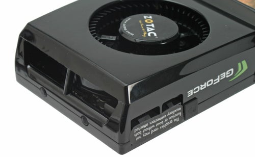
Hidden under rubber flaps along the top of the card are the SLI connectors and an S/PDIF socket. The former enables dual- and triple-SLI configurations and the latter brings the ability to carry digital audio out through the video connections. This supports two-channel LPCM at up to 192KHz, six-channel Dolby Digital at up to 48KHz and DTS 5.1 at up to 96KHz. It doesn’t cover every option, with eight-channel LPCM, Dolby TrueHD and DTS Master Audio being obvious omissions, but it is enough for all but the most elaborate home cinema setups. A DVI-to-HDMI adapter is provided for utilising this.
Outputs are standard fare with two dual-link DVI-I connectors and a seven-pin analogue video connector that supports S-Video natively as well as composite and component via a break-out dongle. Both DVI connections support HDCP encryption so can be used to play back copy-protected HD content like Blu-ray discs.
Video acceleration is the same level as that seen on the 9000-series with H.264, VC-1 and MPEG-2 all benefitting from GPU acceleration. There’s also the questionably useful image post processing, dynamic contrast enhancement, and blue, green and skin tone enhancements that were recently introduced.
One of nVidia’s big marketing campaigns this year has revolved around raising the profile of General Purpose Graphics Processing Unit (GPGPU), the task of performing non-3D-graphics related computation on a GPU. So, with the launch of GT200, nVidia was keen to emphasise the superior GPGPU abilities of its latest chip.
GPUs in general are ideally suited to performing parallel computing tasks, like image manipulation and video conversion, because all those shaders can also be put to task as mini CPUs. Individually they may pale in comparison to a proper CPU but when you’ve got 240 of them, as you have in GT200, the sheer brute force number of shaders will easily out perform any CPU. The big problem at the moment is that writing software to take advantage of parallel processing, and particularly parallel processing on a GPU, is very difficult. This is what prompted nVidia to start working on its CUDA Software Development Kit (SDK), which Hugo recently talked about, and which makes programming for GPGPU considerably easier for the coder.
As well as CUDA as a general programming platform, though, nVidia also recently bought PhysX, the physics processor company, and integrated its technologies into the CUDA SDK. This means that nVidia GPUs can now be put to task in creating life-like physical effects as well as life-like visual effects.
Also, with CUDA being supported by all nVidia’s GPUs since the 8800 GTX, it now has a massive installed user base of 70 million. This has prompted some pretty big name developers to sit up and pay attention to CUDA, including Adobe – it will be using GPU acceleration in its upcoming versions of Photoshop and Premier.
Of course, AMD has also been developing its own competitor to CUDA, in the form of its Close To Metal (CTM) SDK. However, this has had significantly less enthusiastic uptake. Even so, with AMD also planning to support the Havok physics engine and not yet jumping on board with PhysX, the true state of play with regards GPGPU is all very up in the air and personally I’d take the whole thing with a pinch of salt for the time being. That said, for those that are interested, GT200 has made some significant improvements over nVidia’s previous efforts.
Looking at GT200 with regards GPGPU and you have a chip that takes on the following look. The TPCs become mini 24-core processors, each with its own little stores of cache memory. A Thread Scheduler distributes the massive compute load between all the various TPCs and the frame buffer memory acts like main system memory. 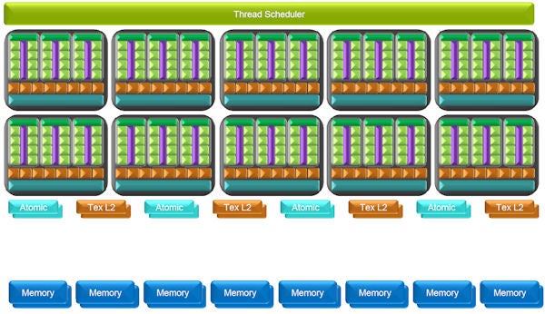
Now in its briefings nVidia went into a lot of detail about why GT200 is better than every nVidia GPU that came before when it comes to GPGPU. However, a lot of the improvement is simply down to the basic increase in processing units rather than any grand new designs. The result is an increase from 518 GigaFLOPs of processing power on G80 to 933 GigaFLOPs on GT200.
That said, there are a few architectural improvements as well. First, thread scheduling has been improved to allow dual-issue MAD+MUL functions to be performed more efficiently. Also double precision (64-bit) calculations are now supported though these rely on 30 (one per SM) dedicated double-precision processors rather than using the SPs themselves, resulting in double-precision performance that is one twelfth that of single-precision (32-bit). Four ‘Atomic’ units have also been added. These are designed to handle particular atomic read-modify-write commands with direct access to memory, rather than utilising the chip’s own caches.
All told, though, it’s a lot of stuff that involves very complicated mathematics, and optimisations thereof, and right now little of it is relevant to the general consumer. When mainstream GPGPU applications begin to hit the shelves we’ll come back to these issues and see what difference they really do make.
So, with all that theory out the way, let’s look at the first consumer card based on GT200, the GTX280.
Taking a further step back we a greeted with the following diagram. 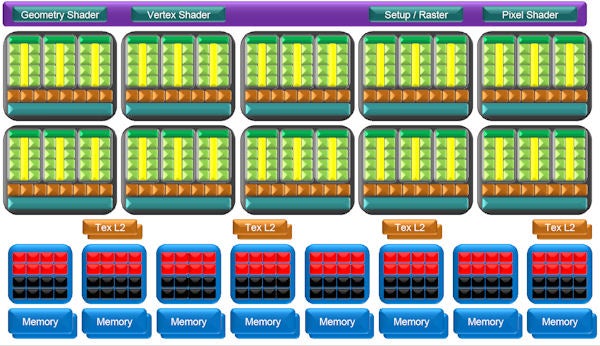
Here we see there are ten TPCs making up the shader-power of the chip in a section that nVidia calls the Streaming Processor Array (SPA). In G80 and G92, the SPA consisted of only eight TPCs, which resulted in the total of 128 SPs. With the increase in SPs per TPC and the increase in TPCs per SPA in GT200, we end up with a total 240 SPs – quite some increase, I’m sure you’d agree. This increase in the number of TPCs also accounts for the improvement in texturing power mentioned earlier. With two extra TPCs you get two extra blocks of texturing units, making for a total of 32 texture address units and 32 texture filtering units, up from 24 of each on G92 and 12 addressing units and 24 filtering units on G80.
Above the SPA is the shader-thread dispatch logic, which manages the task of splitting up the huge number of calculations into TPC sized chunks, as well as the raster / setup engine.
Below the SPA are eight ROP partitions, which handle per pixel tasks like anti-aliasing and alpha-blending. Each ROP partition can process four pixels per clock making for a total of 32 pixels per clock for the whole chip. Also, the new ROPs have been tweaked to enable full speed blending (i.e. 32 pixels per clock) – G80 could only blend 12 and output 24 pixels per clock cycle – so antialiasing, particle effects, shadows, and such like should all see a performance increase with GT200. Each ROP has its own little store of L2 cache memory as well as a dedicated 64-bit connection to the frame buffer making for a total memory interface that’s 512-bits wide. Or in other words, colossal!
Elsewhere there have been a number of tweaks applied that include improved geometry shading and Z-occlusion culling performance. Communication between hardware and driver has also been improved reducing potential bottlenecks that could impact performance.
All told, these changes result in some pretty impressive raw performance figures. Over G80, shader processing power has increased by 87.5 per cent, texturing capabilities by 25 per cent, and pixel throughput by 33.3 per cent. Compared to the dual-chip cards that ATI and nVidia both recently introduced, some of the numbers seem less impressive but there are two things to consider here. First, figures for the dual card solutions assume a perfect doubling up of performance from the two chips involved, which rarely is the case in real life. Secondly, these dual-chip cards only offer performance increases for the games with which they work properly whereas single chip solutions like GT200 will give you a guaranteed level of performance.
So, that’s the logical picture but how does it all relate to that ginormous chip we saw earlier? Well, take a look below. 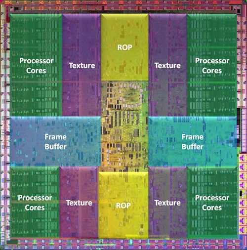
This is a picture of the GT200 with the various compute sections highlighted. The unmarked section in the middle performs a variety of roles but primarily it is concerned with managing the rest of the chip so includes things like the thread scheduler and raster setup.
Finally, one note about DirectX10.1. Put simply, GT200 doesn’t support it, which is a shame. Although 10.1 is only a small tweak that doesn’t bring any new features to Microsoft’s gaming API it does improve efficiency, and thus performance, in certain situations. The only thing in nVidia’s favour here is that few developers are yet utilising these new tweaks. However, this won’t be the case forever. We will just have to wait and see how this one pans out.
It’s quite clear that the nVidia GeForce GTX280 performs superbly and, unlike the recent spate of dual-chip cards we’ve seen, this performance is consistent. Ok, it doesn’t absolutely annihilate everything that came before it, like the 8800 GTX did when it arrived, but there’s a large enough step up that those looking to upgrade their 8800 GTXs have a worthwhile option. Especially as more and more game will become dependent on the extra shader hardware that GT200 provides.
We also like the card’s physical layout with the protective covering of the whole card and LEDs to indicate correct power configuration being welcome additions, while the tried and tested black casing, and a great cooler remain from previous cards. Apart from ATI continuing to have the upper hand when it comes to the way audio pass-through is enabled, we really can’t find fault with the GTX280.
One area where the GTX280 inevitably falls down is in its peak power draw but then it’s only as high as we would expect and is still lower than some cards that have come before it. Take into account the incredibly low idle and video decoding power usage, as well as support for HybridPower and you’ve got a card that shouldn’t worry you too much when it comes to your electricity bill. 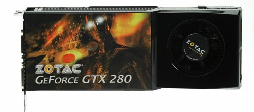
The only factor that really concerns us is price as nVidia has really put the squeeze on, milking every last drop of profit it can while it still has the performance lead. It’s not a surprising move, and we’re sure its competitors would do the same if they had a chance. However, it’s still lamentable. Moreover, while the GTX280 is undeniably the fastest card around, it isn’t that much faster. Certainly not enough to justify paying twice as much as a 9800 GTX. Indeed, were we to recommend anything right now it would be to go and buy two 9800 GTX cards and run them in SLI (a topic we may cover shortly). Either that or wait for our review of the GTX260 to see how that stacks up.
”’Verdict”’
We can find absolutely no fault in the GTX280 when it comes to performance and it has all the features most gamers should care about. Unfortunately, nVidia has played hard ball with the pricing and we simply can’t recommend buying one at the £400 – £450 asking price.
Trusted Score
Score in detail
-
Value 6
-
Features 9
-
Performance 10
Editorial independence
Editorial independence means being able to give an unbiased verdict about a product or company, with the avoidance of conflicts of interest. To ensure this is possible, every member of the editorial staff follows a clear code of conduct.
Professional conduct
We also expect our journalists to follow clear ethical standards in their work. Our staff members must strive for honesty and accuracy in everything they do. We follow the IPSO Editors’ code of practice to underpin these standards.